

XC4010XL-2PC84I
Product Overview
Category
The XC4010XL-2PC84I belongs to the category of programmable logic devices (PLDs).
Use
This product is widely used in digital circuit design and implementation. It provides a flexible and customizable solution for various applications.
Characteristics
- Programmable: The XC4010XL-2PC84I can be programmed to perform specific functions based on the user's requirements.
- High-density: This device offers a high number of logic gates, allowing for complex designs.
- Low power consumption: The XC4010XL-2PC84I is designed to operate efficiently with minimal power consumption.
- Fast operation: With its advanced architecture, this PLD ensures high-speed performance.
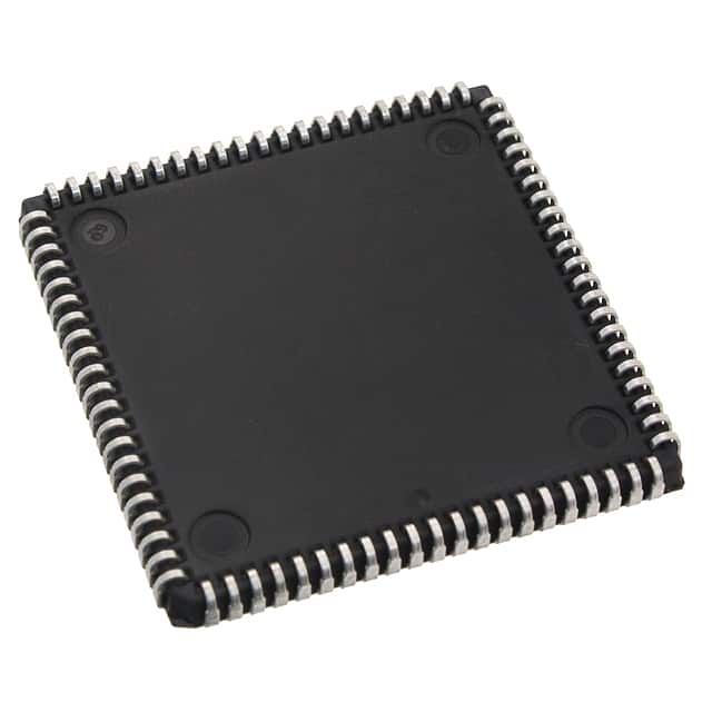
Package
The XC4010XL-2PC84I comes in a compact plastic package that protects the internal components from external factors such as moisture and dust.
Essence
The essence of the XC4010XL-2PC84I lies in its ability to provide reconfigurable logic functions, enabling designers to implement complex digital circuits efficiently.
Packaging/Quantity
This product is typically packaged in reels or trays, with each reel or tray containing a specific quantity of XC4010XL-2PC84I devices. The exact quantity may vary depending on the manufacturer's specifications.
Specifications
- Logic Cells: 400
- Maximum Frequency: 100 MHz
- Operating Voltage: 3.3V
- I/O Pins: 84
- Package Type: Plastic Quad Flat Pack (PQFP)
- Temperature Range: -40°C to +85°C
Detailed Pin Configuration
The XC4010XL-2PC84I has 84 pins, each serving a specific purpose in the circuit design. The pin configuration is as follows:
(Pin Number) (Pin Name) - (Description) 1 - VCCINT - Power supply for internal logic 2 - GND - Ground reference 3 - TCK - Test clock input 4 - TMS - Test mode select 5 - TDI - Test data input 6 - TDO - Test data output 7 - DIN0 - Data input 0 8 - DIN1 - Data input 1 9 - DIN2 - Data input 2 10 - DIN3 - Data input 3 ... 84 - DOUT83 - Data output 83
Functional Features
- Reconfigurable Logic: The XC4010XL-2PC84I allows users to modify the logic functions according to their specific requirements.
- Fast Operation: This PLD offers high-speed operation, enabling efficient execution of complex digital circuits.
- Flexible I/O Configuration: The device provides a range of I/O pins that can be configured to support various interface standards.
- On-Chip Memory: The XC4010XL-2PC84I includes embedded memory blocks, allowing for efficient storage and retrieval of data.
Advantages and Disadvantages
Advantages
- Flexibility: The reconfigurable nature of the XC4010XL-2PC84I makes it suitable for a wide range of applications.
- High-Speed Performance: With its fast operation, this PLD can handle complex designs efficiently.
- Low Power Consumption: The device is designed to minimize power consumption, making it energy-efficient.
Disadvantages
- Limited Resources: The XC4010XL-2PC84I has a finite number of logic cells and I/O pins, which may restrict the complexity of certain designs.
- Programming Complexity: Configuring the device requires expertise in digital circuit design and programming languages.
Working Principles
The XC4010XL-2PC84I operates based on the principles of programmable logic. It consists of a matrix of configurable logic blocks interconnected through programmable interconnects. The user programs the device using hardware description languages (HDL) or design software, specifying the desired logic functions and interconnections. Once programmed, the XC4010XL-2PC84I executes the defined logic operations.
Detailed Application Field Plans
The XC4010XL-2PC84I finds applications in various fields, including:
- Communications: Used in the design of communication systems, such as routers and switches.
- Industrial Automation: Employed in control systems for industrial processes, enabling efficient automation.
- Automotive Electronics: Integrated into automotive electronic systems for functions like engine control and driver assistance.
- Consumer Electronics: Utilized in devices like gaming consoles, set-top boxes, and multimedia players.
- Medical Devices: Incorporated into medical equipment for data processing and control functions.
Detailed and Complete Alternative Models
- XC4028EX-2HQ240C: A higher-density PLD with 4000 logic cells and 240 I/O pins.
- XC9572XL-10VQG44C: A smaller PLD with
قم بإدراج 10 أسئلة وإجابات شائعة تتعلق بتطبيق XC4010XL-2PC84I في الحلول التقنية
Sure! Here are 10 common questions and answers related to the application of XC4010XL-2PC84I in technical solutions:
Q: What is XC4010XL-2PC84I? A: XC4010XL-2PC84I is a field-programmable gate array (FPGA) manufactured by Xilinx.
Q: What are the key features of XC4010XL-2PC84I? A: Some key features include 4000 logic cells, 84-pin plastic quad flat pack (PQFP) package, and 5V operation.
Q: What is the typical power consumption of XC4010XL-2PC84I? A: The typical power consumption is around 500mW.
Q: Can XC4010XL-2PC84I be used for digital signal processing (DSP) applications? A: Yes, XC4010XL-2PC84I can be used for DSP applications as it supports various arithmetic functions and has dedicated hardware resources for DSP operations.
Q: Is XC4010XL-2PC84I suitable for high-speed communication protocols like Ethernet or USB? A: No, XC4010XL-2PC84I does not have built-in support for high-speed communication protocols. Additional external components may be required.
Q: Can XC4010XL-2PC84I be reprogrammed after deployment? A: Yes, XC4010XL-2PC84I is a field-programmable device, which means it can be reprogrammed even after it has been deployed in a system.
Q: What development tools are available for programming XC4010XL-2PC84I? A: Xilinx provides software tools like Vivado or ISE Design Suite for programming and configuring XC4010XL-2PC84I.
Q: What is the maximum clock frequency that XC4010XL-2PC84I can support? A: The maximum clock frequency depends on the specific design and implementation, but it can typically reach frequencies of up to 100 MHz.
Q: Can XC4010XL-2PC84I interface with other components or devices in a system? A: Yes, XC4010XL-2PC84I has various I/O pins that can be used to interface with other components or devices such as sensors, memory, or communication modules.
Q: Are there any limitations or considerations when using XC4010XL-2PC84I in a design? A: Some considerations include limited logic resources compared to newer FPGA models, lack of built-in high-speed communication protocols, and compatibility with older development tools. It's important to review the datasheet and reference designs for specific details and limitations.
Please note that these answers are general and may vary depending on the specific requirements and context of your technical solution.