

XC4010XL-3PC84I
Product Overview
Category
The XC4010XL-3PC84I belongs to the category of Field Programmable Gate Arrays (FPGAs).
Use
FPGAs are integrated circuits that can be programmed and reprogrammed to perform various digital functions. The XC4010XL-3PC84I is specifically designed for applications requiring high-performance logic integration.
Characteristics
- High-performance logic integration
- Programmable and reprogrammable functionality
- Versatile and flexible design options
Package
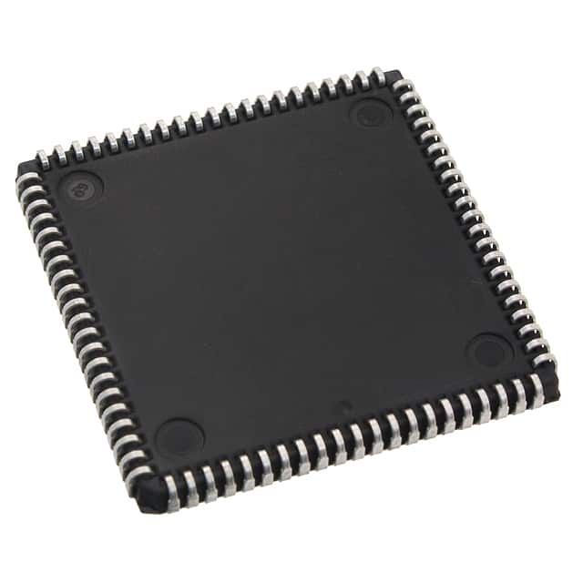
The XC4010XL-3PC84I comes in a 84-pin plastic quad flat pack (PQFP) package.
Essence
The essence of the XC4010XL-3PC84I lies in its ability to provide customizable logic integration, allowing designers to implement complex digital functions on a single chip.
Packaging/Quantity
The XC4010XL-3PC84I is typically packaged in reels or trays, with a quantity of 250 units per reel/tray.
Specifications
- Logic Cells: 4000
- Maximum Frequency: 100 MHz
- Number of I/O Pins: 84
- Operating Voltage: 3.3V
- Programmable Logic Blocks: 40
- Flip-Flops: 1600
- Look-Up Tables: 3200
Detailed Pin Configuration
The XC4010XL-3PC84I has 84 pins, each serving a specific purpose in the overall functionality of the FPGA. The pin configuration includes input/output pins, power supply pins, clock pins, and configuration pins. A detailed pinout diagram can be found in the product datasheet.
Functional Features
- High-speed performance
- Configurable logic cells
- Flexible I/O options
- On-chip memory blocks
- Dedicated clock management resources
Advantages and Disadvantages
Advantages
- Customizable logic integration
- Reconfigurable functionality
- High-performance capabilities
- Versatile design options
Disadvantages
- Steep learning curve for beginners
- Limited resources compared to ASICs
- Higher power consumption compared to dedicated hardware solutions
Working Principles
The XC4010XL-3PC84I operates based on the principles of configurable logic. It consists of programmable logic blocks, flip-flops, look-up tables, and interconnect resources. The user can program the FPGA using a Hardware Description Language (HDL) to define the desired digital functions and interconnections.
Detailed Application Field Plans
The XC4010XL-3PC84I finds applications in various fields, including: 1. Telecommunications: Implementing signal processing algorithms, protocol handling, and data compression. 2. Industrial Automation: Controlling and monitoring complex systems, such as robotics and manufacturing processes. 3. Aerospace and Defense: Performing high-speed data processing, radar signal analysis, and encryption/decryption. 4. Medical Devices: Enabling real-time image processing, patient monitoring, and diagnostics. 5. Automotive: Implementing advanced driver assistance systems, engine control units, and infotainment systems.
Detailed and Complete Alternative Models
- XC4028XLA-3HQ240C: A higher-capacity FPGA with 4000 logic cells and 240-pin package.
- XC9572XL-10VQG44C: A smaller FPGA with 72 logic cells and 44-pin package.
- XC6SLX45-2FGG484C: A more advanced FPGA with 45,000 logic cells and 484-pin package.
These alternative models offer different capacities, pin configurations, and performance levels to suit specific project requirements.
In conclusion, the XC4010XL-3PC84I is a versatile FPGA that provides high-performance logic integration for various applications. Its customizable nature, along with its functional features and advantages, make it a valuable tool for digital design engineers.
قم بإدراج 10 أسئلة وإجابات شائعة تتعلق بتطبيق XC4010XL-3PC84I في الحلول التقنية
Sure! Here are 10 common questions and answers related to the application of XC4010XL-3PC84I in technical solutions:
Q: What is XC4010XL-3PC84I? A: XC4010XL-3PC84I is a field-programmable gate array (FPGA) manufactured by Xilinx.
Q: What are the key features of XC4010XL-3PC84I? A: Some key features include 4000 logic cells, 84-pin plastic quad flat pack (PQFP) package, and 3.3V power supply.
Q: What is the typical application of XC4010XL-3PC84I? A: XC4010XL-3PC84I is commonly used in various digital design applications such as telecommunications, industrial control systems, and consumer electronics.
Q: How can I program XC4010XL-3PC84I? A: XC4010XL-3PC84I can be programmed using Xilinx's proprietary software called ISE Design Suite.
Q: Can XC4010XL-3PC84I be reprogrammed after it has been programmed once? A: Yes, XC4010XL-3PC84I is a reprogrammable FPGA, which means it can be reprogrammed multiple times.
Q: What is the maximum operating frequency of XC4010XL-3PC84I? A: The maximum operating frequency of XC4010XL-3PC84I depends on the specific design and implementation, but it can typically operate at frequencies up to several hundred megahertz.
Q: Does XC4010XL-3PC84I support different voltage levels? A: No, XC4010XL-3PC84I operates on a fixed 3.3V power supply and does not support different voltage levels.
Q: Can XC4010XL-3PC84I interface with other components or devices? A: Yes, XC4010XL-3PC84I can interface with other components or devices through its I/O pins, which can be configured as inputs or outputs.
Q: Are there any limitations or constraints when using XC4010XL-3PC84I? A: XC4010XL-3PC84I has certain limitations such as limited logic resources and I/O pins, so it is important to carefully plan and optimize the design to meet the requirements.
Q: Where can I find more information about XC4010XL-3PC84I? A: You can find more detailed information about XC4010XL-3PC84I in the datasheet provided by Xilinx or by referring to Xilinx's official documentation and support resources.