

XC4013XL-2PQ208C
Product Overview
Category
The XC4013XL-2PQ208C belongs to the category of programmable logic devices (PLDs).
Use
This product is commonly used in digital circuit design and implementation. It provides a flexible and customizable solution for various applications.
Characteristics
- Programmable: The XC4013XL-2PQ208C can be programmed to perform specific functions based on user requirements.
- High-density: It offers a high number of logic elements, allowing for complex designs.
- Low power consumption: The device is designed to operate efficiently with minimal power consumption.
- Fast operation: The XC4013XL-2PQ208C provides high-speed performance, enabling quick execution of logic operations.
Package
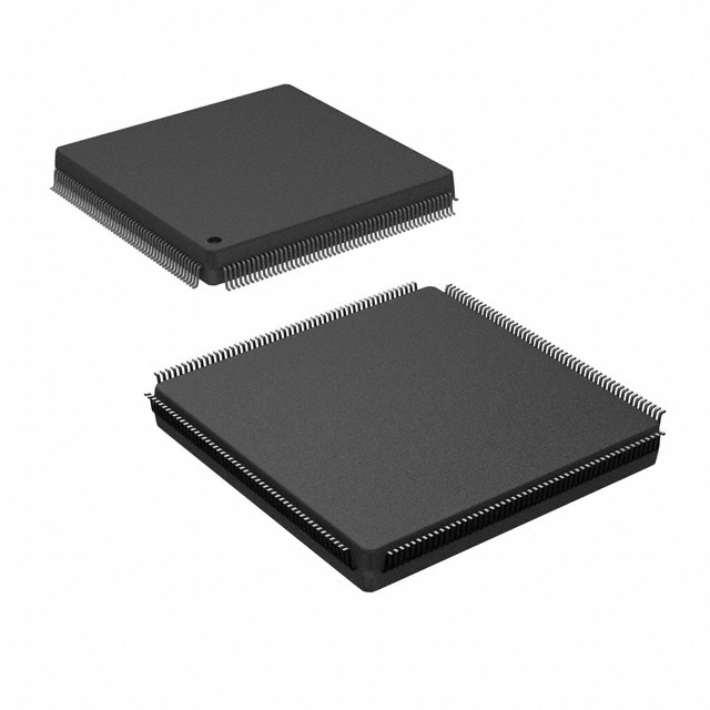
The XC4013XL-2PQ208C comes in a PQ208 package, which refers to a plastic quad flat pack with 208 pins.
Essence
The essence of the XC4013XL-2PQ208C lies in its ability to provide reconfigurable logic functionality, allowing users to implement custom digital circuits without the need for dedicated hardware.
Packaging/Quantity
The XC4013XL-2PQ208C is typically packaged individually and is available in various quantities depending on the supplier.
Specifications
- Logic Elements: The XC4013XL-2PQ208C offers 4000+ logic cells, providing ample resources for complex designs.
- I/O Pins: It features 100+ input/output pins, facilitating communication with external devices.
- Operating Voltage: The device operates at a voltage range of 3.3V to 5V, ensuring compatibility with different systems.
- Speed Grade: The XC4013XL-2PQ208C is available in multiple speed grades, allowing users to choose the appropriate one based on their application's requirements.
Detailed Pin Configuration
The XC4013XL-2PQ208C has a total of 208 pins, each serving a specific purpose. The pin configuration is as follows:
- Pin 1: VCCIO - Power supply for I/O banks
- Pin 2: GND - Ground reference
- Pin 3: TCK - Test clock input
- Pin 4: TMS - Test mode select
- Pin 5: TDI - Test data input
- ...
- Pin 208: NC - No connection
For a complete pin configuration diagram, please refer to the product datasheet.
Functional Features
The XC4013XL-2PQ208C offers several functional features that enhance its usability and performance:
- Reconfigurability: The device can be reprogrammed multiple times, allowing for iterative design improvements.
- Embedded Memory: It includes on-chip memory elements, enabling storage of intermediate results or configuration data.
- Clock Management: The XC4013XL-2PQ208C supports various clocking options, allowing precise control over timing requirements.
- I/O Flexibility: It provides a wide range of I/O options, including differential signaling and voltage compatibility.
Advantages and Disadvantages
Advantages
- Flexibility: The XC4013XL-2PQ208C offers unparalleled flexibility in designing digital circuits, accommodating a wide range of applications.
- Cost-effective: By eliminating the need for dedicated hardware, it reduces overall system costs.
- Time-saving: The programmable nature of the device allows for rapid prototyping and faster time-to-market.
Disadvantages
- Complexity: Utilizing the full potential of the XC4013XL-2PQ208C requires expertise in digital circuit design and programming.
- Limited Resources: Despite its high-density capabilities, the device may have limitations when dealing with extremely complex designs.
Working Principles
The XC4013XL-2PQ208C operates based on the principles of field-programmable gate arrays (FPGAs). It consists of an array of configurable logic blocks interconnected through programmable routing resources. These logic blocks can be programmed to perform specific functions, and the interconnections can be configured to establish desired signal paths.
Upon programming, the XC4013XL-2PQ208C executes the defined logic operations, enabling the realization of complex digital circuits.
Detailed Application Field Plans
The XC4013XL-2PQ208C finds applications in various fields, including:
- Communications: It can be used for protocol conversion, data encryption/decryption, and signal processing in communication systems.
- Industrial Automation: The device enables the implementation of control systems, motor control, and sensor interfacing in industrial automation setups.
- Automotive Electronics: It can be utilized for engine management, driver assistance systems, and infotainment systems in automobiles.
- Medical Devices: The XC4013XL-2PQ208C can contribute to medical imaging, patient monitoring, and diagnostic equipment
قم بإدراج 10 أسئلة وإجابات شائعة تتعلق بتطبيق XC4013XL-2PQ208C في الحلول التقنية
Sure! Here are 10 common questions and answers related to the application of XC4013XL-2PQ208C in technical solutions:
Question: What is XC4013XL-2PQ208C?
Answer: XC4013XL-2PQ208C is a specific model of Xilinx FPGA (Field-Programmable Gate Array) that offers programmable logic capabilities for various technical applications.Question: What are the key features of XC4013XL-2PQ208C?
Answer: Some key features of XC4013XL-2PQ208C include 4000 Logic Cells, 192 I/O pins, 32Kbits of Block RAM, and support for various communication protocols.Question: What are the typical applications of XC4013XL-2PQ208C?
Answer: XC4013XL-2PQ208C can be used in a wide range of applications such as industrial automation, telecommunications, automotive electronics, medical devices, and more.Question: How do I program XC4013XL-2PQ208C?
Answer: XC4013XL-2PQ208C can be programmed using Xilinx's Vivado Design Suite or ISE Design Suite software tools, which allow you to design and implement your desired logic functions.Question: Can XC4013XL-2PQ208C be reprogrammed after deployment?
Answer: Yes, XC4013XL-2PQ208C is a reprogrammable FPGA, meaning you can modify its configuration even after it has been deployed in a system.Question: What power supply requirements does XC4013XL-2PQ208C have?
Answer: XC4013XL-2PQ208C typically operates at a voltage range of 3.3V, but it also supports other voltage levels depending on the specific application requirements.Question: Can XC4013XL-2PQ208C interface with other components or devices?
Answer: Yes, XC4013XL-2PQ208C has multiple I/O pins that can be used to interface with other components or devices such as sensors, actuators, memory modules, and more.Question: Are there any limitations or constraints when using XC4013XL-2PQ208C?
Answer: XC4013XL-2PQ208C has certain limitations such as limited logic resources, limited memory capacity, and specific timing constraints that need to be considered during design.Question: Can XC4013XL-2PQ208C handle real-time processing tasks?
Answer: Yes, XC4013XL-2PQ208C is capable of handling real-time processing tasks, but the complexity and performance will depend on the specific requirements of the application.Question: Where can I find additional resources or support for XC4013XL-2PQ208C?
Answer: You can refer to Xilinx's official website, user guides, datasheets, forums, and online communities for additional resources and support related to XC4013XL-2PQ208C.