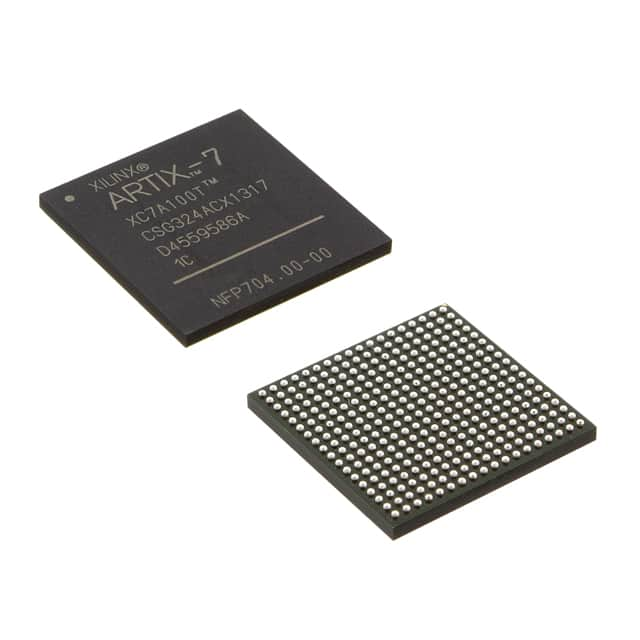
XC7A100T-2CSG324C
Product Overview
Category
The XC7A100T-2CSG324C belongs to the category of Field Programmable Gate Arrays (FPGAs).
Use
FPGAs are integrated circuits that can be programmed after manufacturing. The XC7A100T-2CSG324C is specifically designed for high-performance applications, such as digital signal processing, embedded systems, and high-speed communication.
Characteristics
- High performance: The XC7A100T-2CSG324C offers a high logic capacity and fast processing speeds.
- Flexibility: Being programmable, it allows for customization and adaptability to various applications.
- Reconfigurability: The FPGA can be reprogrammed multiple times, making it suitable for prototyping and iterative development.
- Parallel processing: FPGAs excel at parallel processing tasks, enabling efficient execution of complex algorithms.
Package and Quantity
The XC7A100T-2CSG324C comes in a 324-ball grid array (BGA) package. It is typically sold individually or in small quantities.
Specifications
- Logic Cells: 101,440
- Flip-Flops: 202,880
- Block RAM: 4,860 Kbits
- DSP Slices: 240
- Maximum Frequency: 600 MHz
- I/O Pins: 210
Pin Configuration
For a detailed pin configuration diagram of the XC7A100T-2CSG324C, please refer to the manufacturer's datasheet.
Functional Features
The XC7A100T-2CSG324C offers several functional features that enhance its performance and usability:
- High-speed interfaces: It supports various high-speed serial protocols, such as PCIe, Gigabit Ethernet, and USB.
- Integrated memory blocks: The FPGA includes dedicated memory blocks for efficient data storage and retrieval.
- DSP capabilities: The XC7A100T-2CSG324C incorporates digital signal processing (DSP) slices, enabling efficient implementation of complex algorithms.
- Configurable I/O standards: It supports a wide range of I/O voltage standards, allowing compatibility with different devices.
- Partial reconfiguration: The FPGA allows specific sections to be reprogrammed while the rest of the design remains operational.
Advantages and Disadvantages
Advantages
- High performance and processing speeds.
- Flexibility and adaptability to various applications.
- Parallel processing capabilities.
- Reconfigurability for iterative development.
- Support for high-speed interfaces and integrated memory blocks.
Disadvantages
- Steep learning curve: Utilizing FPGAs requires specialized knowledge and expertise.
- Higher power consumption compared to dedicated ASICs.
- Relatively higher cost compared to microcontrollers or general-purpose processors.
Working Principles
FPGAs are based on a matrix of configurable logic blocks (CLBs) interconnected by programmable routing resources. The XC7A100T-2CSG324C utilizes look-up tables (LUTs) within the CLBs to implement desired logic functions. These LUTs can be programmed to create custom digital circuits.
The configuration of the FPGA is stored in non-volatile memory, which is loaded during startup. Once configured, the FPGA operates as per the programmed logic, executing tasks in parallel and providing high-performance computing capabilities.
Application Field Plans
The XC7A100T-2CSG324C finds applications in various fields, including:
- Digital Signal Processing: Its high-performance capabilities make it suitable for implementing complex DSP algorithms used in audio and video processing, telecommunications, and radar systems.
- Embedded Systems: FPGAs are commonly used in embedded systems for their flexibility and ability to interface with different peripherals and protocols.
- High-Speed Communication: The XC7A100T-2CSG324C supports high-speed serial interfaces, making it ideal for applications requiring fast data transfer, such as networking equipment and data centers.
Alternative Models
For alternative models with similar capabilities, consider the following options:
- XC7A200T-2CSG324C: Offers higher logic capacity and performance.
- XC7K160T-2FBG676I: Provides additional features like integrated transceivers for high-speed communication.
Please refer to the manufacturer's website or datasheets for detailed specifications of these alternative models.
In conclusion, the XC7A100T-2CSG324C is a high-performance FPGA that offers flexibility, parallel processing capabilities, and support for various high-speed interfaces. Its applications range from digital signal processing to embedded systems and high-speed communication. While it requires specialized knowledge and has higher power consumption compared to other solutions, its reconfigurability and performance make it a valuable choice for demanding applications.
قم بإدراج 10 أسئلة وإجابات شائعة تتعلق بتطبيق XC7A100T-2CSG324C في الحلول التقنية
Sure! Here are 10 common questions and answers related to the application of XC7A100T-2CSG324C in technical solutions:
Q: What is XC7A100T-2CSG324C? A: XC7A100T-2CSG324C is a field-programmable gate array (FPGA) manufactured by Xilinx. It belongs to the Artix-7 family and has 101,440 logic cells.
Q: What are the key features of XC7A100T-2CSG324C? A: Some key features include a high-performance FPGA fabric, integrated block RAM and DSP slices, multiple I/O standards, and low power consumption.
Q: What are the typical applications of XC7A100T-2CSG324C? A: XC7A100T-2CSG324C is commonly used in various applications such as industrial automation, automotive electronics, telecommunications, medical devices, and aerospace systems.
Q: How can XC7A100T-2CSG324C be programmed? A: XC7A100T-2CSG324C can be programmed using Xilinx's Vivado Design Suite, which provides a comprehensive development environment for FPGA designs.
Q: What is the maximum operating frequency of XC7A100T-2CSG324C? A: The maximum operating frequency of XC7A100T-2CSG324C depends on the specific design and implementation, but it can typically reach frequencies of several hundred megahertz.
Q: Can XC7A100T-2CSG324C interface with other components or devices? A: Yes, XC7A100T-2CSG324C supports various communication protocols such as UART, SPI, I2C, Ethernet, and PCIe, allowing it to interface with a wide range of components and devices.
Q: What is the power consumption of XC7A100T-2CSG324C? A: The power consumption of XC7A100T-2CSG324C depends on the specific design and utilization, but it typically operates at low power levels, making it suitable for energy-efficient applications.
Q: Can XC7A100T-2CSG324C be used in safety-critical systems? A: Yes, XC7A100T-2CSG324C can be used in safety-critical systems. It offers features like built-in error detection and correction mechanisms, making it suitable for applications with high reliability requirements.
Q: Are there any development boards available for XC7A100T-2CSG324C? A: Yes, Xilinx provides development boards like the Arty A7-100T, which are specifically designed to support XC7A100T-2CSG324C and facilitate prototyping and development.
Q: Where can I find additional resources and support for XC7A100T-2CSG324C? A: Xilinx's website offers comprehensive documentation, application notes, reference designs, and a community forum where you can find additional resources and get support for XC7A100T-2CSG324C.


