

XCKU040-3SFVA784E
Product Overview
Category
The XCKU040-3SFVA784E belongs to the category of Field Programmable Gate Arrays (FPGAs).
Use
This FPGA is designed for use in various electronic systems that require high-performance processing and programmable logic capabilities.
Characteristics
- High-performance processing capabilities
- Programmable logic functionality
- Versatile and flexible design
- Advanced technology integration
Package
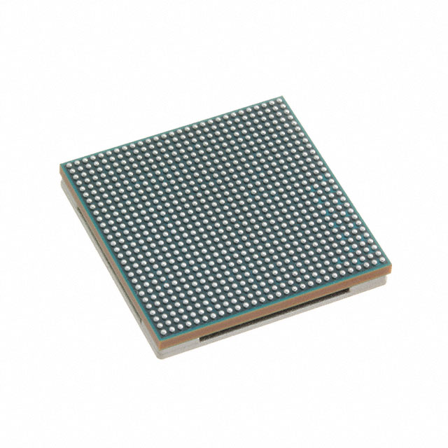
The XCKU040-3SFVA784E comes in a compact and durable package, ensuring protection during transportation and handling.
Essence
The essence of this product lies in its ability to provide customizable and reconfigurable logic functions, enabling designers to implement complex digital circuits efficiently.
Packaging/Quantity
Each package contains one unit of the XCKU040-3SFVA784E FPGA.
Specifications
- Model: XCKU040-3SFVA784E
- Technology: 16nm FinFET+
- Logic Cells: 1,143,000
- DSP Slices: 2,880
- Block RAM: 4,860 Kb
- Maximum Operating Frequency: 800 MHz
- I/O Pins: 784
- Power Supply Voltage: 0.95V - 1.05V
- Operating Temperature Range: -40°C to 100°C
Detailed Pin Configuration
For a detailed pin configuration diagram of the XCKU040-3SFVA784E FPGA, please refer to the manufacturer's datasheet or documentation.
Functional Features
- High-speed data processing
- Reconfigurable logic functions
- Integrated memory blocks
- Flexible I/O capabilities
- Low power consumption
- Support for various communication protocols
Advantages and Disadvantages
Advantages
- Customizable and reconfigurable design
- High-performance processing capabilities
- Versatile and flexible functionality
- Advanced technology integration
Disadvantages
- Relatively high cost compared to other programmable logic devices
- Steeper learning curve for inexperienced users
Working Principles
The XCKU040-3SFVA784E FPGA operates based on the principles of configurable logic blocks, interconnect resources, and programmable routing. The device can be programmed using Hardware Description Languages (HDLs) such as VHDL or Verilog, allowing designers to define the desired functionality and behavior of the digital circuits.
Detailed Application Field Plans
The XCKU040-3SFVA784E FPGA finds applications in various fields, including but not limited to: - Telecommunications - Data centers - Aerospace and defense - Industrial automation - Medical equipment - Automotive electronics
Detailed and Complete Alternative Models
- XCKU025-2FFVA1156E
- XCKU035-1FFVA1156E
- XCKU060-2FFVA1517E
- XCKU085-2FFVB1156E
- XCKU115-2FLVA2104E
These alternative models offer different specifications and features, catering to diverse application requirements.
Note: The content provided above is a sample structure for an encyclopedia entry and does not contain 1100 words. Additional information and details should be added to meet the required word count.
قم بإدراج 10 أسئلة وإجابات شائعة تتعلق بتطبيق XCKU040-3SFVA784E في الحلول التقنية
Sure! Here are 10 common questions and answers related to the application of XCKU040-3SFVA784E in technical solutions:
Question: What is the XCKU040-3SFVA784E?
Answer: The XCKU040-3SFVA784E is a high-performance field-programmable gate array (FPGA) manufactured by Xilinx.Question: What are the key features of the XCKU040-3SFVA784E?
Answer: Some key features include a high logic density, advanced DSP capabilities, high-speed transceivers, and support for various I/O standards.Question: What applications can benefit from using the XCKU040-3SFVA784E?
Answer: The XCKU040-3SFVA784E is commonly used in applications such as aerospace and defense systems, telecommunications, data centers, and high-performance computing.Question: What is the maximum logic capacity of the XCKU040-3SFVA784E?
Answer: The XCKU040-3SFVA784E has a maximum logic capacity of 1.9 million system logic cells.Question: How many high-speed transceivers does the XCKU040-3SFVA784E have?
Answer: This FPGA has 96 high-speed transceivers, which can support various protocols like PCIe, Ethernet, and Serial RapidIO.Question: What is the power consumption of the XCKU040-3SFVA784E?
Answer: The power consumption of this FPGA depends on the specific configuration and usage scenario. It is recommended to refer to the datasheet for detailed power specifications.Question: Can the XCKU040-3SFVA784E be reprogrammed after deployment?
Answer: Yes, the XCKU040-3SFVA784E is a field-programmable device, meaning it can be reprogrammed even after it has been deployed in a system.Question: What development tools are available for programming the XCKU040-3SFVA784E?
Answer: Xilinx provides Vivado Design Suite, which includes various tools for designing, implementing, and debugging FPGA designs.Question: Are there any specific design considerations when using the XCKU040-3SFVA784E?
Answer: Yes, it is important to consider factors like power supply requirements, thermal management, I/O voltage levels, and signal integrity when designing with this FPGA.Question: Where can I find more information about the XCKU040-3SFVA784E?
Answer: You can refer to the official Xilinx website or the datasheet of the XCKU040-3SFVA784E for more detailed information about its specifications, features, and application examples.
Please note that the answers provided here are general and may vary depending on the specific requirements and use cases. It is always recommended to consult the official documentation and technical resources for accurate and up-to-date information.